

 Favorite (7)
Microsystemstechnology is a subfield of microtechnology, focusing on education, research, development, and production of microsystems. Significant overlaps exist between various subfields concerning integration technology and its applications, making it challenging to categorize individual components. The different subfields and their intersections are illustrated in the following graphic.
.png?format=.jpg&upscale=False&x=1164)
MEMS, short for Microelectromechanical Systems, is a process technology used to create small systems that combine mechanical components (such as levers, springs, membranes, chambers, or channels) with electrical components (such as resistors, capacitors, and inductors). This combination allows for detection, control, and execution at a micro level, which can have impacts on a macro scale. The MEMS field encompasses a wide range of disciplines, including:
When optical functions are integrated with mechanical and electronic components, the systems are referred to as "Micro Opto Electro Mechanical Systems" (MOEMS). Optical communication has proven to be an effective solution for addressing network scalability issues caused by the exponential increase in data traffic due to the rapid growth of the Internet. Current routing technology slows the flow of information (or bits) by converting optical signals to electronic information and then back to light before transmission. All-optical networks offer significantly better throughput and performance compared to conventional electronic systems. Key MOEMS products include waveguides, optical switches, cross-connects, multiplexers, filters, modulators, detectors, attenuators, and equalizers. The small size, low cost, low power consumption, mechanical durability, high precision, high switch density, and cost-effective batch processing of these MEMS-based devices make them ideal for managing and switching optical signals in telecommunication networks.
MEMS for biomedical applications are often referred to as BioMEMS. RF-MEMS (Radio-Frequency Microelectromechanical Systems) is another rapidly growing subfield of MEMS technologies. These systems are specifically developed for electronics in communication applications such as mobile phones, radar, GPS, and steerable antennas. RF-MEMS technology includes components for circuit tuning (capacitors, inductors, resonators, filters, microphones, and switches). These RF functions are low-loss, ultra-small, and highly integrative. As RF-MEMS components continue to replace traditional components in today's mobile phones, devices could become extremely small (the size of a wristwatch is within reach), require very little battery power, and be more affordable. RF-MEMS has thus enabled improved performance, reliability, and functionality of these devices while reducing their size and cost.
The complexity of MEMS is evident in the wide range of markets and applications it encompasses. MEMS are utilized in nearly every aspect of life, including the automotive industry, medicine, electronics, communication, and the security and defense sectors. This makes MEMS one of the most crucial technologies of the 21st century.
.png?format=.jpg&upscale=False&x=1164)
The history of Microelectromechanical Systems (MEMS) highlights their diversity, challenges, and applications. Emerging from research labs in the early 1950s, MEMS have continuously evolved and are now integral to a variety of products and applications.
In the 1950s, foundational developments in MEMS began, including the introduction of the first silicon strain gauges in 1958. A pivotal moment was Richard Feynman's famous 1959 lecture, "There is Plenty of Room at the Bottom", at the California Institute of Technology, where he proposed numerous ideas for technology at the microscopic level. His suggestions later formed the basis of nanotechnology, offering a $1,000 reward for creating an electric motor smaller than 1/64 inch.
The 1960s saw significant advancements, such as the demonstration of the first silicon pressure sensor in 1961 and Westinghouse's invention of surface micromachining and the Resonant Gate Field Effect Transistor (RGT) in 1967. This invention enabled the release of micromechanical devices from the silicon substrate using sacrificial material-based processes. The 1970s brought further breakthroughs, including the first silicon accelerometer in 1970 and the development of the first micromachined inkjet nozzle in 1979.
In the early 1980s, experiments with surface-micromachined silicon began. The late 1980s saw growing interest in micromachining, benefiting especially the microelectronics industry. 1982 was notable for the introduction of the disposable blood pressure transducer and the publication of the seminal paper "Silicon as a Mechanical Material," which served as a reference for silicon's material properties and etching data. This paper highlighted the advantages of silicon as a mechanical material and the relevant mechanical properties and processing techniques for micromechanical structures, guiding the scientific community in handling silicon in MEMS. Additionally, the LIGA process was developed in 1982, and the first MEMS conference was held in 1988.
In the 1990s, micromachining methods focused on improving sensors. The Multi-User MEMS Process (MUMPS) was launched by MCNC in 1992, sponsored by the Defense Advanced Research Projects Agency (DARPA). In 1993, Analog Devices sold the first surface-micromachined accelerometer (ADXL50), and deep reactive ion etching (DRIE) was patented in 1994. From the mid-1990s, MEMS components began appearing in commercial products, such as accelerometers for airbag control in vehicles, pressure sensors for medical applications, and inkjet printheads. BioMEMS experienced rapid development starting in 1995, followed by MEMS optical network components in the early 2000s. Today, MEMS are found in a wide range of applications, from projection displays to data storage systems, with the greatest potential in telecommunications (optical and wireless), biomedicine, and process control.
This historical development illustrates not only the versatility and potential of MEMS but also the numerous challenges overcome to integrate this technology into everyday life.
As previously mentioned, MEMS consist of various combinations of mechanical (levers, springs, membranes, combs, channels) and electrical (resistors, capacitors, inductors, etc.) components that function as sensors or actuators. Generally, MEMS are composed of four elements, all integrated onto a single chip:
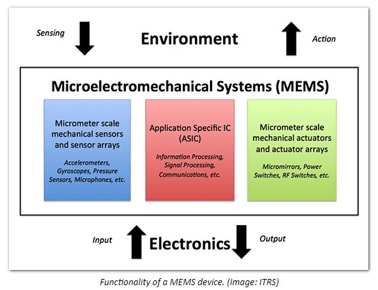
MEMS can function as sensors, receiving information from their environment and providing an electrical output signal, or as actuators, which convert an electrical signal into an action. Both sensors and actuators are known as transducers, as they convert one form of signal or energy into another. A typical MEMS device combines a microelectromechanical sensor or actuator packaged together with an integrated circuit (IC). The IC serves as the electrical interface to the sensor or actuator, facilitating signal processing/compensation and providing an analog or digital output.
While the IC utilizes the electrical properties of silicon, MEMS take advantage of other material properties such as optical, mechanical, thermal, magnetic, and chemical characteristics. An overview of the functioning of MEMS is illustrated in the following graphic.
Microelectromechanical components are created through advanced manipulation of silicon and other substrates using micromachining processes. The fabrication of MEMS often employs the same methods and tools used in integrated circuit (IC) production, such as deposition, photolithography, and etching. While conventional macroscopic manufacturing techniques like injection molding, turning, and drilling are effective for producing three-dimensional (3D) shapes and objects, they may be limited in small-scale applications due to their low complexity.
In MEMS fabrication, batch processing similar to large-scale IC production is applied, where two-dimensional (2D) layers are added or removed from a substrate (typically silicon) through photolithography and chemical etching. The 3D aspect of MEMS components results from the structuring and interaction of these 2D layers. Additional layers can be incorporated through various thin-film and bonding techniques, as well as by etching sacrificial "spacer" layers.
The MEMS technology has adapted some of these IC manufacturing techniques for specific applications and introduced new processes to create mechanical devices such as microfluidic channels, gears, cantilevers, micromotors, comb drives, and gyroscopes. These techniques used in MEMS fabrication are also known as micromaterial processing and are detailed below.
Most laser micromachining processes are not parallel and therefore not fast enough for effective MEMS manufacturing. However, they are useful for specialized micromachining or mold-making. Unlike the batch fabrication technologies used for integrated circuits, the MEMS industry does not have a generic technology platform akin to the semiconductor industry. On the contrary, there are dozens of MEMS product groups, each containing several distinct products tailored for specific applications and markets. Each of these product groups relies on its own often unique technology.
Despite the promising potential of MEMS technologies, several challenges currently hinder their widespread adoption. Most companies that could benefit from this technology lack the necessary skills and expertise to support MEMS manufacturing. Designing a MEMS component requires a high level of manufacturing knowledge, and significant time and money are invested during the development and prototyping phases. To boost innovation and creativity while reducing unnecessary market entry costs, advanced simulation and modeling tools are essential for accurately predicting the behavior of MEMS components.
Currently, there is no generic packaging solution for MEMS, as each device requires a specific format. As a result, packaging is the most expensive manufacturing step, often accounting for 90% (or more) of the final cost of a MEMS component. Due to the relatively small number of commercial MEMS components and the rapid pace of technological development, standardization has been very challenging. High-quality control and basic forms of standardization are generally found only in facilities with multi-million (or billion) dollar investments.
Another challenge is education and training in the MEMS field. The complexity and interdisciplinary nature of MEMS require well-educated scientists and engineers from various backgrounds. In times of skill shortages and declining numbers of trainees and students in STEM fields, finding qualified personnel is difficult.
Despite these challenges, MEMS technology offers several critical advantages as a manufacturing technology, including its interdisciplinary nature and wide range of applications. This diversity has led to an unprecedented array of devices and synergies in previously unrelated fields, such as biology and microelectronics. MEMS enable the creation of components and devices with higher performance and reliability, along with the obvious benefits of smaller physical size, reduced volume, lower weight, and lower cost. Additionally, MEMS provide the basis for manufacturing products that cannot be produced by other methods. These factors make MEMS a potentially more widespread technology than integrated circuit microchips.
However, many challenges and technological barriers related to miniaturization must be addressed and overcome before MEMS can realize their full potential. IVAM is supporting this by connecting professionals in these high-tech industries and helping them in bringing innovative technologies and products to market and gaining a competitive edge.
